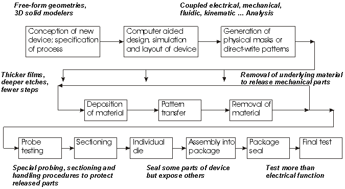
Figure 1. MEMS technology builds from the basic silicon ICs manufacturing process flow. Some of the significant distinctions between MEMS and ICs are noted in bold italics. Source: Electronics Technology Office, DARPA.
MicroElectroMecahnical Systems (MEMS) are integrated micro devices or systems combining electrical and mechanical components that can sense, control, and actuate on the micro scale and function individually or in arrays to generate effects on the macro scale. MEMS is one of the most promising areas in future computer and machinery, the next logical step in the silicon revolution. Fabricated using Integrated Circuit (IC) compatible batch-processing techniques, the small size of MEMS opens a new line of exciting applications, including aerospace, automotive, biological/medical, fluidics, military, optics, and many other areas. Reliability is of concern if MEMS machinery is used in critical applications. MEMS is usually a combination of circuits and micro-machinery. The reliability aspect includes both the electronic and the mechanical parts, complicated by the interactions. Different from mechanical systems, inertia is of little concern; the effects of atomic forces and surface science dominate. Wafer Level Reliability (WLR) has received increasing interest in recent years. We still have limited knowledge on how MEMS devices fail. Limited tools and models are available. How to model the reliability of MEMS is a challenge.
MicroElectroMechanical systems (MEMS) are integrated micro devices or systems combining electrical and mechanical components fabricated using Integrated Circuit (IC) compatible batch-processing techniques and range in size from micrometers to millimeters. These systems can sense, control, and actuate on the micro scale and function individually or in arrays to generate effects on the macro scale. [MCNC99]
Technology has been pushed to the point that we can build machinery so small that it can not be seen by human eye. The typical size of MEMS devices is usually measured in micrometers or even microns. Using similar fabrication techniques as building microprocessors, we are now able to build sensors and actuators on the same microscopic level with the processor chip. Measured in microns, thermal sensors, pressure sensors, inertial sensors, flow and viscosity sensors, resonators, levers, gears, transmission systems, micro-mirrors, valves, pumps, motors, ... can be batch produced together on the same chip with the processing unit. They indeed compose a "system on a chip".
A whole new line of applications are opened up by this fast developing technology, limited maybe only by imagination. We can now make medical and biomedical devices so small that they can be injected into humans' bloodstream. They may selectively kill sick cells or germs, leaving healthy body tissue intact. They may intelligently monitor blood substance and release drugs whenever necessary. "Microsurgery" is assigned a new meaning by intelligent MEMS devices. Controlled by outside central computers, MEMS microsurgery devices can do surgery inside human body without any cut on the skin. One day they may even be able to do DNA processing and sequencing right on site.
Controlled chemical reactions at microscopic level are also possible with MEMS technology. Miniature valves, pumps make it possible to build a chemical plant on a chip. New substances can be made when needed and a very fine grain control can be achieved.
Devices in many existing applications are facing the challenge of mass-fabricated, low-cost MEMS devices. At a relatively small fraction of the cost, size and weight of these systems, MEMS substitutes may even perform much better than their traditional counterparts. MEMS accelerometers that deploy airbags during a car-crash, and the inkjet-printer cartridges that can inject fine drops of ink on paper to form letters or graphs have been widely used. MEMS displays are very power-efficient and have very high definitions. Storage devices can achieve density up to terabytes per square centimeter. [Garbriel98]
Traditional material and mechanical science is being revolutionized and rejuvenated. Polysilicon is still the prevailing material used in both mechanical parts and electronic parts in MEMS devices. VLSI fabrication technique has advanced to build mechanical components together with electronic components. Issues like strength, tear and wear, corrosion, are new challenging topics.
Just like IC technology 30 years ago, MEMS technology is still in its juvenile age. Most of the MEMS products are still prototypes. How MEMS devices would fail is not very well understood. At microscopic level, assumptions in macroscopic level will not always hold. Factors that can be ignored in macro scale become important in micro scale. Without sufficient attention on these factors, reliability and quality of MEMS devices can be so impaired that they are unusable or even destroyed the moment after fabrication. Reliability is the hindering factor to prevent commercialization and utilization of MEMS device in critical applications.
Today most of the present MEMS products are still prototypes, but MEMS is the next logical step in the silicon revolution. With a $10 Billion market today, and an estimated market of $34 Billion market in the year 2002, [Micromachine97] advances in reliability is a dominating factor to evolve from prototypes to real-world applications, from infancy to maturity.
The challenging issue in MEMS technology development and commercialization is justifying its reliability. The reliability issues of MEMS devices are more than a simple combination of electrical reliability, material reliability and mechanical reliability. Fabricating multiple devices on the same chip will have to deal with more failure modes. Complex interactions of cross-domain signals, interference and substances induce new failure modes. For sensor inputs, the chip will have to be exposed to some environmental stimuli, such as heat, humidity, vibration, etc. The input and output voltage may not be within the 5 volts range of standard IC. Some actuators need hundreds of volts to operate. And for microfluidic devices, there might be chemicals and fluids flowing around the chip, with higher potential for corrosion.
Many MEMS device failures are introduced in the fabrication process, and many failure modes in operation are related to the fabrication process. Being miniature embedded systems themselves, MEMS devices are usually batch fabricated using a process similar to those used in IC technology, using silicon wafers as the material and etching techniques to build components. Both MEMS fabrication and IC fabrication share the same characteristics such as mass-production, low cost, products fabricated completely assembled without piece parts. But the MEMS fabrication process is more complicated, as it has to have mechanical parts and electro-mechanical parts integrated with electronic parts on the same die. They usually have more complex shapes, have moving joints and pivots, need more material strength, and may even need lubrication.
The manufacturing process flow is shown in Figure 1. The distinctions between MEMS and ICs are in bold italics. In the design phase, complex CAD tools having the ability to model complex 3D objects have to be used for MEMS. The challenge is the simultaneous modeling of devices in many domains, including electronic, mechanical, chemical, and the ability to analyze cross-domain effects.
Figure 1. MEMS technology builds from the basic
silicon ICs manufacturing process flow. Some of the significant distinctions
between MEMS and ICs are noted in bold italics. Source: Electronics Technology
Office, DARPA.
In the cycle from material deposition to material removal, mechanical parts need special attention. Mechanical parts may have complex shapes and may require material with special strength, such as the joint of the gear, and will have mechanical parts that can move freely, such as the lever or the gear chain. So the film of material deposited must be thick enough to form the mechanical layer. The process is repeated multiple times until the required device is constructed. Moving parts can be released after etching away the silicon dioxide layer.
Common processing techniques that are used to sculpt mechanical structures include bulk micromachining, wafer-to-wafer bonding, surface micromachining, and high-aspect ratio micromachining. Bulk micromachining is the term applied to a variety of etching procedures that selectively remove material, typically with a chemical etchant whose etching properties are dependent on the crystallographic structure of the bulk material. Wafer-to-wafer bonding is a strategy commonly employed to get around the restrictions in the type of structures that can be fabricated using bulk micromachining. Because anisotropic etching, by definition, only removes material, bonding of wafers allows for the addition of material to the bulk micromachining repertoire. High-aspect ratio micromachining is a newer technique, allow the fabrication of thick (usually greater than hundreds of microns and up to centimeters thick), precision, high-aspect ratio MEMS structures (structures with near-vertical sides). In surface micromachining (SMM), alternating layers of structural (usually Polysilicon) and sacrificial material (usually silicon dioxide) are deposited and etched to form the shape required. Surface micromachining enables the fabrication of free-form, complex and multi-component integrated electromechanical structures, giving freedom to fabricate devices and systems without constraints on materials, geometry, assembly and interconnections that is the source for the richness and depth of MEMS applications that cut across so many areas. More than any other factor, it is surface micromachining that has ignited and is at the heart of the current scientific and commercial activity in MEMS. [Gabriel98]
Testing is very important for quality and reliability purposes. Testing MEMS devices is unique. Compared to electronic devices, that have electric voltage/current as input and electric voltage/current as output, MEMS devices may have a closed loop -- from sensors to actuators. The input can be temperature, humidity, loudness, acceleration ... and the output can be various electrical or mechanical responses. Testing MEMS devices require the proper setup of inputs and accurate measure of the outputs.
Packaging is the Achilles' heel of MEMS manufacturing. Unlike IC packaging, MEMS packaging is an application-specific task and can completely destroy a potential product's ability to reach the marketplace. MEMS packages must have the ability to meet at least one or more of the following criteria:
Following the same path taken in IC technology, Wafer Level Reliability (WLR) has received increasing interest in recent years. Polysilicon is the major material used to construct both the electric and mechanical parts of MEMS devices. It is an ideal material, not only because it is the most abundant solid element in the Earth's lithosphere, but also because of its high strength. [Petersen82] Researchers have found that at least presently, material strength is not a key limiting factor in MEMS performance and reliability, [Miller98] i.e. fracture, wear and tear of the material are not the dominant causes of MEMS failures. The material can endure sustained high stress so that it can be used in joints, beams and springs. However, failures induced by wear can be found in parts that involve sliding motion and operate in stress. [Peterson98] [Miller98a] Little evidence was found in support of corrosion wear. Surface fatigue, deformation and impact wear typically require forces in excess of those for abrasive wear. Again such forces were not applied. Fretting wear occurs where machine elements experience fluctuating loads, leading to microcracks and fatigue failure. They have not been observed. [Miller98a]
In [Peterson98], some common MEMS failures are found in the study of microengines.
Particles could naturally be expected to have a detrimental mechanical or electrical effect on devices where small gaps exist between bearing surfaces or elements with large potential differences. Particulate contamination has been a minor problem. The particles which receive attention are those which might be internally generated, or present in spite of a clean room environment.
A condition that results from overdriving, leading to inadvertent contact of structural and electrical members has been observed in springs and in comb fingers. Overdriving occurs when large voltages are applied.
Sticking occurs between contacting surfaces. It can affect even elements that are not powered.
Evidence has been found to show that clamping of gears due to electrostatic charges are present at certain energy levels, preventing the gears from moving. In the study of [Brown96], a summary of common failure modes for MEMS structures include:
Many MEMS operate at stress levels in the vicinity of 1 GPa. In several cases high stresses are necessary to overcome stiction in membrane geometries. These stress levels are higher by at least one order of magnitude than macroscopic structures. Small defects that act as critical cracks at these stress levels can be introduced by etching, polishing, or rough handling.
High stresses can be associated with multilayer films, introduced by processing, thermal mismatch, or epitaxial mismatch. The adhesion between layers depends strongly on their chemical and mechanical compatibility.
High stresses and stress gradients introduce the possibility of time-dependent mass transfer through glide and diffusion mechanisms. Although the creep strains that result are negligible macroscopically, they can be enormous on the scale of MEMS. The increasing use of metal as a structural material in MEMS where room temperature creep exists should be of concern to MEMS manufacturers.
MEMS are designed for a variety of applications where environmental effects can be important. This includes valves, sensors, and pumps where the contacting fluids, including water, can be corrosive. Experiments have shown that crack growth is a function of moisture. [Brown97]
Cyclic loading of MEMS couples with the previously described mechanisms associated with static loading, creep and environmental effects. Any process that results in an irreversible repositioning of atoms within a material can contribute to fatigue. There is evidence that fatigue life of Polysilicon is a function of stress. [Brown97] In all the failure modes observed, stiction and friction are of serious concern. Stiction is the mechanism by which released MEMS structures are attracted and stick to each other. [Miller98] The generic route to failure observed for all rotating devices involves sticking of structures that are in sliding contact. The observed time-dependent routes to failure involve changes that occur in rubbing surfaces. Rotating devices typically exhibit intermittent sticking of rubbing surfaces, with the frequency of sticking increasing until the engine pinion gear no longer exhibits complete rotation, and finally ceases to move at a sticking position. These changes are accelerated by excessive lifetime. [Miller97] Friction welding has also been observed in the binary counter. [Peterson98]
Most of the root causes of the failure modes observed are different from the common causes in macroscopic level. For example, gravitational forces are negligible. The dominant forces are associated with contacting or rubbing surfaces. Some root causes [Miller98] are:
The final step in the process of fabricating surface micromachined MEMS is a wet chemical etch, which removes the silicon dioxide matrix that encapsulates the moveable mechanical structures. Removal of the wafer from the liquid etchant results in a meniscus (liquid-air interface) that often pulls moveable structures into contact via capillary forces. Once in contact, and even after drying, the surfaces often remain in contact due to various types of adhesion forces (e.g. capillary, van Der Walls, electrostatic due to trapped charge). Further, stiction can happen even without liquid. Surfaces brought into contact after successful drying can still adhere, resulting in impaired functionality or failure. Moreover, when microscopic surfaces are exposed to such uncontrolled environments as air with changing humidity or packages with epoxy vapors, their properties can change significantly (typically for the worse).
MEMS actuators usually contain physically constrained systems. For example, the motion of the gear is constrained by the hub on which it rotates, and the comb drives are constrained by the linkages connecting them to the pinion gear. All the forces associated with the system balance to result in the dynamical behavior of the system. Control is provided by the actuating electrical drive signals. If appropriate drive signals are not provided, significant constraint forces can result to compensate for other forces, such as inertia. Constraint forces, particularly of the type associated with rubbing surfaces, are observed to result in premature failure. It is thus desirable to operate MEMS in a way that minimizes forces between rubbing surfaces. Experiments show that MEMS actuators driven by model-based drive signals have 5 orders of magnitude longer life than square wave signals. So improper operational methods, i.e. those not using drive signals compatible to the operational model designed to minimize parasitic constraint forces, can significantly degrade performance and reliability of MEMS. Consequently, the method of operation must be seriously considered when developing MEMS that are to be highly reliable.
Microelectromechanical systems are just that: micromechanical devices typically actuated by electrical forces. Electrical forces such as capacitive attraction can depend sensitively on the geometry of the attracting electrodes, and must be carefully considered when implementing constraint methods for moving mechanical elements. Otherwise, undesired forces can result in mechanical instabilities causing both performance degradation and premature failure. For example, lateral clamping occurs when the comb drive shuttle is not perfectly aligned, causing the support springs to buckle in the lateral direction.
In addition to the degradation in performance (the time-dependent position of the output gear deviates from the desired path), lateral clamping directly results in two distinct types of failures. First, the abrupt angular acceleration experienced by the gear during each revolution results in severe parasitic frictional forces between the gear and the hub on which it rotates, as well as in the pin joint connecting the gear to the linkage arm. The excessive force between the rubbing surfaces causes the gear to bind on the hub, and rotation to cease. The second failure mode occurs when an individual comb drive finger deflects sufficiently to contact an adjacent finger. When this occurs, the two typically fuse together, causing immediate and abrupt failure of the comb drive.
The successful implementation of model-based operational methods requires a knowledge of the relationship between the applied voltage (or current) and the resulting actuation force. If this relationship deviates from that used in creating model-based drive signals, unexpected forces result that can have devastating consequences. A deviation from the expected force-voltage relationship can result from parasitics associated with the complex 3-dimensional shape of interacting actuation electrodes. For example, experiments have unambiguously demonstrated that the increase in force of the comb drive at large displacement is due to fringing fields at the ends of the comb fingers that occur when the combs are fully engaged. The increased force causes the pinon gear to accelerate as the comb drives become fully engaged. The gear then abruptly comes to a halt as the combs remain engaged. The electrostatic field energy favors this "linearly clamped" condition, where the system is in a local potential energy well. Motion resumes only when the applied voltage drops below the unclamping value. As with lateral clamping, the speed fluctuations associated with linear clamping not only impact the positional accuracy of the actuation system, but result in premature degradation as well. When the electrostatic drive forces do not properly compensate the other forces in the system, constrain forces acting on rubbing or otherwise contacting surfaces result in wear and premature failure. In particular, the gear begins sticking at the 135° and 270° position, and eventually ceases motion at one of those two positions.
The challenge of MEMS design tools is the ability to do full-scale 3-D modeling, and cross-domain modeling of mixed devices. Some of the design tools are listed at http://mems.mcnc.org/technet/designtools.html.
Almost all the failure analysis techniques in IC can be used in MEMS FA. In [Peterson98], a complete listing of failure analysis techniques are provided.
Optical microscopy is one of the most valuable and widely used tools in the
FA of MEMS. In addition to permitting observations of the obvious, such as
which elements are functioning properly and verification of the failures, it
can provide a quick initial view of small defects. The features that can be
observed optically include textures, stains, debris, fracture, and abnormal
displacements.
Scanning laser microscopy has been used primarily to obtain confocal images.
A confocal image is an image with a very limited depth of field (depth of
focus) created by inserting an aperture in the optical path. By taking a series
of confocal images at different focal planes, an extended depth-of-focus image
can be constructed. The extended depth-of-focus image is particularly useful in
resolving elements which have abnormal vertical displacements.
The SEM has been useful for imaging defects at high magnification as well as
determining electrical continuity in static and operating microengines. Passive
and active voltage contrast techniques have identified structures at potentials
different from those expected. Passive voltage contrast is defined as contrast
which arises from voltage differences induced by rastering the beam causing
various elements reach an equilibrium potential through self-charging. Active
voltage contrast is defined as that arising from external application of
voltage on different structures. In both cases, contrast is generated by
differences in secondary electron emission yields caused by differences in
surface potential. When imaging with a primary beam energy of 1keV, areas that
are at positive potential appear dark in the images and those that are at
ground appear bright. It has been possible, by increasing the accelerating
potential, to observe a polarity change in the features which were charging,
due to a crossover in the secondary electron emission efficiency.
The focused ion beam (FIB) uses a 30 keV beam of positive gallium ions (Ga
+ ) to irradiate the surface of the sample in a defined
area. This irradiation causes surface charging, which can be neutralized by a
flow of low energy (~ 30 eV) electrons from a flood gun. Images can be made
using a signal consisting of either secondary ions or secondary electrons with
or without charge neutralization by the electron flood gun. The FIB has been
used to image structures, to cross section elements of concern and to cut
elements free for subsequent examination.
The atomic force microscope (AFM) provides very detailed topographic images
and surface traces.
Infrared microscopy is often used to construct thermal images based on the
infrared radiance emitted from the structures. Hot spots can be found using
infrared microscopy.
Light emission testing is a common technique used in FA of ICs. Like many
other techniques, it can also be used in the FA of MEMS devices.
Acoustic microscopy was employed on stationary microengines in an attempt to
resolve contact between stuck gears and links and the substrate. This technique
is more destructive to the sample due to the introduction of water as a
coupling fluid. The acoustic signal could not be translated into evidence of
sticking, although morphological features were resolved.
Acoustic emission was also evaluated on several engines while they were
running. This involved the attachment of a sensor to the package containing the
microengines and "listening" for acoustic events as microengines were
operated. No signal was resolvable above the background noise level.
A laboratory laser cutter has been used to excise portions of circuits and
sever connections to determine which elements are free or stuck. It has also
been used to impart energy to members such as gears and links which moves like
a shock wave to agitate discrete portions of the overall system.
Careful removing elements of a microengine with a conductive laboratory adhesive tape used for SEM mounting has added another dimension to the analysis of microengines. The lift-off technique allows examination of the bottom surfaces of engines (Fig. 23) that provide additional information (such as the accumulation of wear debris or evidence of damage to pin receiver holes) for determining failure modes of the defective and failed microengines.
Once MEMS failure modes are identified, techniques targeted to eliminate the corresponding problems can be used to improve the reliability of MEMS devices.
Stiction is a major cause of the failures of MEMS devices. A liquid echant
used in fabrication process can cause moving parts to stick when dried.
Hydrophobic coating and improved release etches and drying schemes such as
super-critical CO2 drying have done much to lessen its impact. While coupling
agents and other coating materials are being investigated to reduce stiction,
the long-term effectiveness remains largely unexplored. The development of
manufacturable methods to stabilize the properties of surfaces is critical to
the continued commercialization of MEMS products.
Constraint forces can result in overstress and wear-out of the parts.
Improper operational methods, i.e. those not using model-based drive signals
designed to minimize parasitic constraint forces, can significantly degrade
performance of MEMS. Consequently, the method of operation must be seriously
considered when developing MEMS that are to be highly reliable.
Clever design modifications to the parts that fail frequently can improve its reliability and prolong its life. Thickness, stiffness, and shape, etc are typical factors of concern. For example, lateral clamping can be mitigated by changing the shape of the interface between the alignment guides and the comb shuttle. Specifically, the gaps at the ends of the comb fingers when they are fully engaged are made large enough that the parasitic force due to the end fringing fields is negligible.
Failure models for MEMS are scarce. It is critical that a failure model be developed that describes the physics of failure and allows prediction of ultimate failure in any final design. [Miller98a] provides an Adhesive Failure Model capable of predicting failures in actual use, on the assumption that adhesive wear is the most likely prevalent mechanism responsible for failure in the micromachines.
MEMS technology is a fast enabling technology and a cross-disciplinary subject that has relationships to many areas.
Traditional reliability theory and electronic/electrical reliability theory still apply to MEMS reliability analysis. Above that more issues also have to be considered, such as the interactions between electronic, electric and mechanical components.
The mechanical reliability of MEMS device is of great concern. First Polysilicon is the major material used for mechanical parts. More study has to be done on how it performs and fails in MEMS devices. Second it is not a direct analogy from the real-world mechanical reliability, because assumptions used in macro scale may not hold in micro scale. Other forces and factors become dominant.
MEMS itself is a miniature embedded system itself, a "system on a chip". It gives new architecture choices for old applications as well as opens a new line of applications.
Sensors, actuators are tightly coupled on the same chip with the processing unit. Redesign and reimplementation of traditional sensors and actuators in MEMS has special impact on future applications.
MEMS technology will merge the functions of compute, communicate and power together with sense, actuate and control to change completely the way people and machines interact with the physical world. Using an ever-expanding set of fabrication processes and materials, MEMS will provide the advantages of small size, low power, low mass, low cost and high functionality to integrated electromechanical systems both on the micro as well on the macro scale. [DARPA vision] The market is booming. Micromachined accelerometers are now being used as sensors for airbag actuation in over 50% of the new cars being built [Payne98]. Texas Instruments has commercialized its Digital Micromirror Device (DMD) which is being used in tens of thousands of bright projection displays worldwide. [Miller98a]
MEMS will open up a broad new array of cost-effective solutions only if they prove to be sufficiently reliable. [Miller98a] In order to rapidly take advantage of this technology, reliability must be considered concurrently with technology development. Current research shows that failures induced by deficiencies in material/mechanical properties are not the majority, such as fracture strength or fatigue-related fracture. Failure causes are typically related to contacting or rubbing surfaces: Stiction and friction-related wear. Corresponding measures to minimize those failures can be taken to improve MEMS reliability. Chemical surface treatments are effective against sticking after drying of liquid echant. Model-based operational methods [Miller98] can minimize parasitic forces, eliminate overstress and wear-out of critical parts. Clever design modifications will rule out some common failures observed.
MEMS technology is still in its infancy, like IC technology 30 years ago. Focus has been put in wafer level reliability, the same path taken in the IC technology. Presently how MEMS fail is still not well understood. Available tools and techniques are mostly improvised versions from IC tools. Reliability models are scarce.
[Gabriel98] pictures the state-of-art and future trends of MEMS technology development, shown in Figure 2.
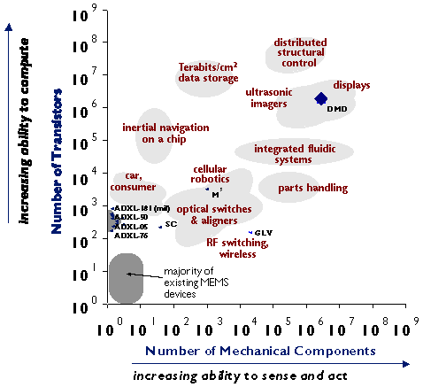
Figure 2: Log-log plot of number of transistors merged with number of mechanical components for MEMS devices and systems. The resulting map represents a quantitative way to measure and track MEMS technology advances across different application areas.
Website of MEMS Technology Applications Center (MCNC). A short overview of MEMS technology is provided. Definition of MEMS, introduction of fabrication processes, and more.
The DARPA MEMS program and vision website. Gives overview, appication areas and impact of MEMS. The short-term and long-term goal of DARPA MEMS program are also discussed in detail.
An athorative introductory to MEMS technology. MEMS devices, fabrication, application, market trends and future directions are discussed. Good tutorial material.
In this short 2-page paper reliability and long-term stability of MEMS are briefly discussed and the potential failure modes for MEMS structures are intorudced. The paper is short but rich in information.
"Traditional fatigue testing method is used in MEMS testing, using resonant fatigue secimens. Fatigue life of Polysilicon is found to be a function of stress. The time-dependent failure may be corrosion fatigue of the native oxide on the surface of the Polysilicon specimen."
"We identify failure modes common to a broad range of MEMS actuators, including adhesion (stiction) and friction-induced failures caused by improper operational methods, mechanical instabilities, and electrical instabilities. Demonstrated methods to mitigate these failure modes include implementing optimized designs, model-based operational methods, and chemical surface treatments."
Elaborates MEMS fabrication technology in concert with IC fabrication technology.
Failure causes for devices in sliding friction. Conventional failure modes such as fatigue induced fracture did not occur, indicating that the devices are mechanically extremely robust. The generic route to failure observed for all rotating devices involves sticking of structures that are in sliding contact. This sticking evidently results from microscopic changes in the sliding surfaces during operation. The rate at which these changes occur is accelerated by excessive applied forces, which originate from non-optimized designs or inappropriate drive voltages. Precursors to failure are observed, enabling further understanding of the microscopic changes that occur in the sliding surfaces that ultimately lead to failure.
Microelectronic failure analysis (FA) has been an integral part of the development of state-of-the-art integrated circuits. FA of MicroElectroMechanical Systems (MEMS) is moving from its infancy to assume an important role in the successful design, fabrication, performance and reliability analysis for this new technology. The primary failure mode we have identified is directly related to visible wear on bearing surfaces. In this paper, we describe in detail the characteristics of the failure modes in binary counters. We also compare the failure characteristics with those of an earlier version of the microengine.
A detailed discussion about MEMS reliability. A valid reliability assessment of MEMS has three prerequisites: 1. statistical significance 2. a technique for accelerating fundamental failure mechanisms and 3. valid physical models to allow prediction of failures during actual use. These already exist for the microelectronics portion of such integrated systems. The challenge lies in the less well-understood mi-cromachine portions and its synergistic effects with microelectronics. This paper presents a methodology addressing these prerequisites and a description of the underlying physics of reliability for micromachines.
Possibilities to use silicon to build mechanical parts.
Gives MEMS application areas and numbers about MEMS market.
Tutorials:
Academics and research:
These links give comprehensive lists of internet MEMS resources:
http://qa-web.jpl.nasa.gov/quality/aip/mems.html-ssi
http://www.mdl.sandia.gov/micromachine/links.html
http://www.mdl.sandia.gov/micromachine/biblog_general.html
A list of bibliographies. With full paper available. http://hypatia.dartmouth.edu/levey/ssml/links1.html
A comprehensive link to other related MEMS and micro-fabrication sites.
http://mems.isi.edu/ MEMS clearing house
http://mems.mcnc.org/memshome.html
Picture gallery.