My research in this area began in 1989, when Marco Racanelli (presently vice-president at Jazz Semiconductor) and I built the first working UHV/CVD reactor outside of IBM. The UHV/CVD technique had been invented by Bernie Meyerson in 1986 and is particularly suited to germanium-silicon heterostructures because of its low growth temperature. Published work from this period included the reactor construction; growth rate measurements and theory of the growth rate kinetics; layer uniformity; doping with n type and p type impurities; and some results on heterojunction bipolar transistors.
With Richard Strong, Ramesh Misra, and Sanjay Vyas I began working on structures suitable for infrared detectors. Published work concerns both heterojunction internal photoemission and quantum well infrared photodetector structures (QWIP). Photoluminescence and diffraction studies were performed to evaluate the quality of QWIP structures. TEM and SIMS was important in understanding undesired boron doping in HIP structures. Ultimately we concluded from FTIR that QWIP structures did not exhibit strong intersubband absorption in normal incidence, and consequently we focused on the HIP structure. These structures were fabricated into detectors and measurements suggest that they will offer background-limited performance in the long-wave infrared region when operated at 40 K or below. Anda Mocuta explored the incorporation of carbon into germanium-silicon alloys and fabricated and characterized p-channel heterostructure MOSFETs.
Other work concerned growth of structures for heterojunction bipolar transistors and was part of a DARPA-funded MAFET program at Northrup Grumman.
I have written a number of review articles on germanium-silicon epitaxy.
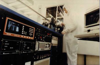
1. Photograph of the UHV/CVD reactor (dismantled in 2001)
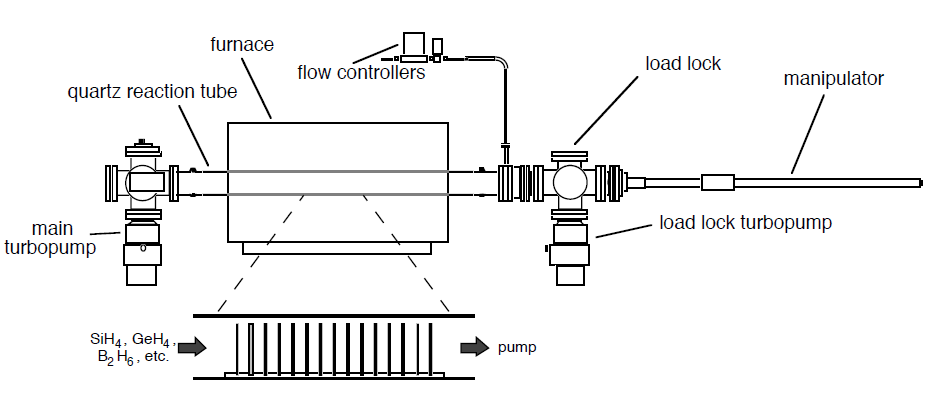
2. Schematic diagram of the UHV/CVD reactor
\