This work was conducted in collaboration with
Randy Feenstra, Art Smith, Vidhya Ramachandran, and Huajie Chen
(all of the Department of Physics)
The objective was to study the surface reconstructions when GaN or related materials are grown on sapphire or SiC substrates, and to use this knowledge to understand and improve the epitaxial growth process. We reported the first atomic-resolution images of the GaN surface.
One of the STM photographs from this system was on the cover of Science magazine for August 14, 1998.
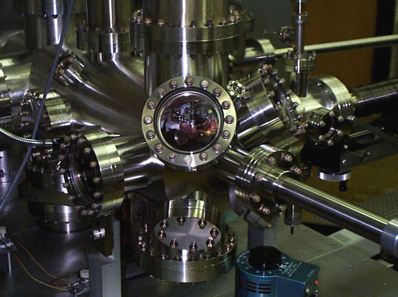
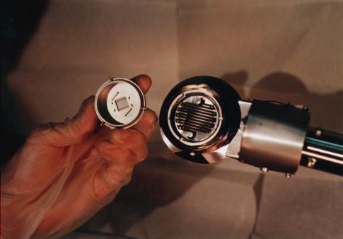
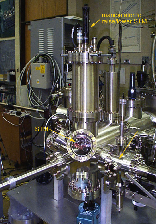
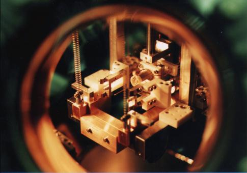
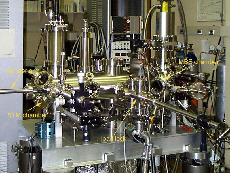
This research was performed in a specially designed MBE system which permits in situ scanning probe microscopy. Some pictures of the system are shown below.
Pictures of the MBE/STM system are found below:
1. Overall view of the system
2. View of the MBE chamber