1000 Hz
100 kHz
10 MHz
(funded by the NSF XYZ-on-a-chip program, September, 2000)
The goal of this project is the development of low-cost sensing systems capable of multiple simultaneous analyses of biological systems. These sensing systems will be applied to the electronic detection of cell motion and/ or cell division. Information obtained electronically will be used directly or in combination with microscopic techniques. Sensing is based on the use of large-area microelectronic fabrication techniques, which will ensure low cost, disposability, redundancy, accuracy, and high speed data collection. A direct interface with digital electronics will facilitate rapid analysis and throughput at least an order of magnitude higher than existing techniques (which will lead to improved productivity in pharmaceutical and biological research).
We have developed an array for live cell screening (referred to as LCAST, for Live Cell Array Sensing Technology) which will make it possible to perform direct electrical sensing of cell motility and/or division. At present, optical sensing is used in cell proliferation and screening studies; individual cells are placed in wells on a partitioned plastic substrate. In this methodology, cells are exposed to drugs or other reagents and the response of the cell is observed microscopically. Each experimental site is analyzed sequentially, which involves microscope translation, focus, and complex image processing. In our approach thousands of sites will be interrogated electronically for cell activity. Electrical sensing will increase the data rate, facilitate direct computer analysis, and reduce the number of lost cells. This sensor will have applications in combinatorial cell biology where, for example, the effects of cytokines and other molecular factors on cellular motility and/or proliferation rate can be tested.
The work was conducted at two institutions: Carnegie Mellon University (Pittsburgh, PA) and Lehigh University (Bethlehem, PA). Carnegie Mellon is the lead institution for this program. Lehigh University received a subcontract from Carnegie Mellon. Lehigh worked on developing a TFT technology for the active-matrix array. Carnegie Mellon performed biological experiments on medium-sized electrodes; modeled the effect of cells on the electrode impedance; performed several biological experiments using medium-sized electrodes fabricated at Carnegie Mellon; designed a CMOS active matrix chip; developed techniques for post-processing the CMOS chip; and demonstrated the use of the active matrix array to address individual cell-sized electrodes.
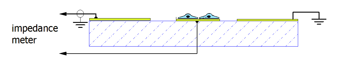
The figure below shows the sensing concept, originally
proposed by Giaever and Keese. The electrical impedance is measured between a
small sensing electrode and a large counter-electrode.
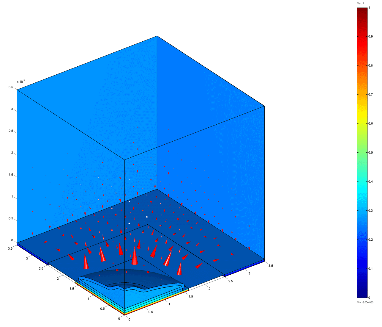
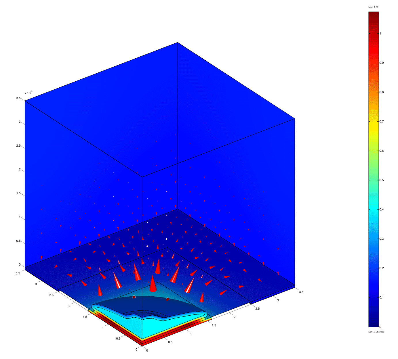
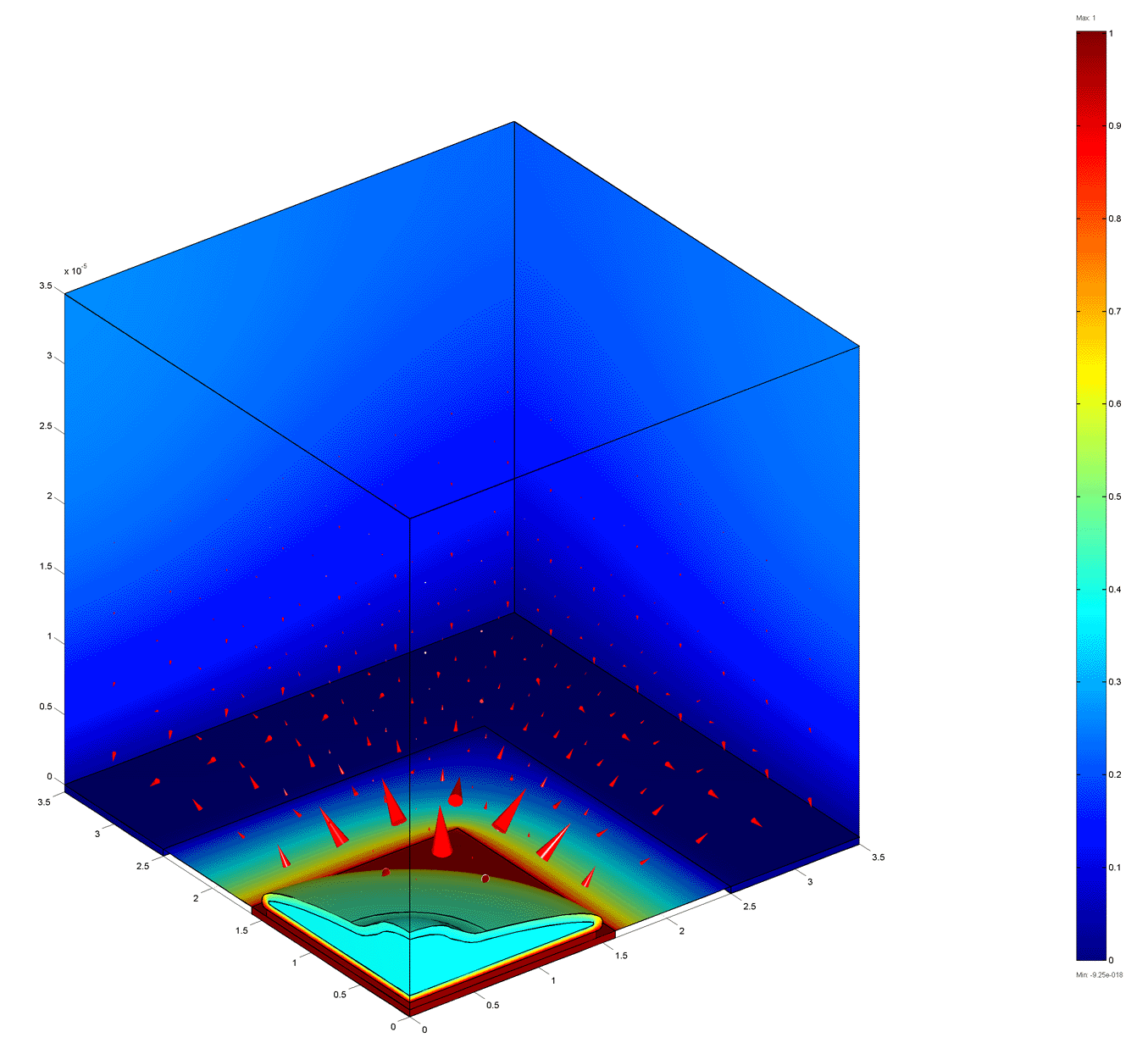
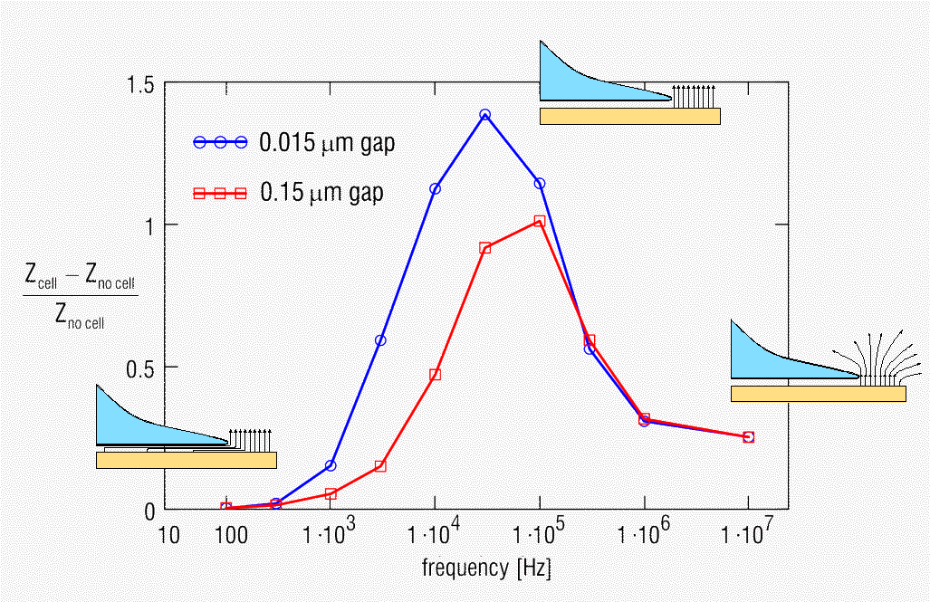
The figures below show the electric potential (colors) and current density (arrows) for a cell on an electrode at various frequencies. Current flows laterally beneath the celll at low frequencies. The cell blocks the current flow at intermediate frequencies. At high frequencies the impedance is largely due to spreading resistance which is weakly dependent on the cell coverage.
The simulated impedance magnitude change as a function of frequency is shown in the figure below for two values of the cell-electrode gap.
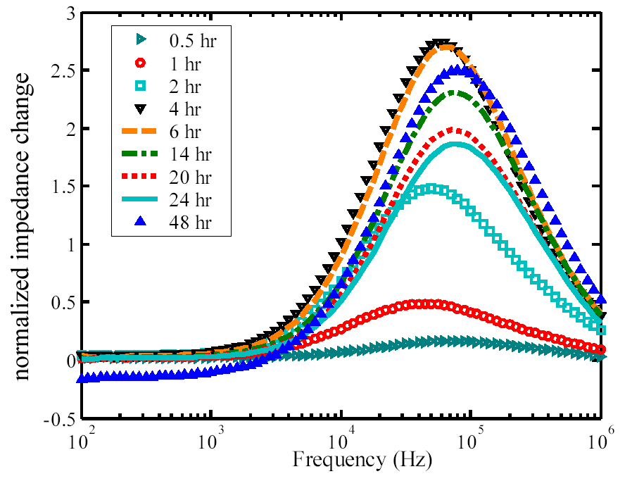
The next figure shows the measured normalized impedance
change as a function of frequency for fibroblasts on an electrode as a function
of time after dosing the cells.
This basic approach has been used to perform a number of
biological experiments as detailed in our publications. Some of the conference
proceedings paper drafts are linked from our publication
list.
A particular goal of this project is the fabrication of an active matrix array. Several figures are presented below.
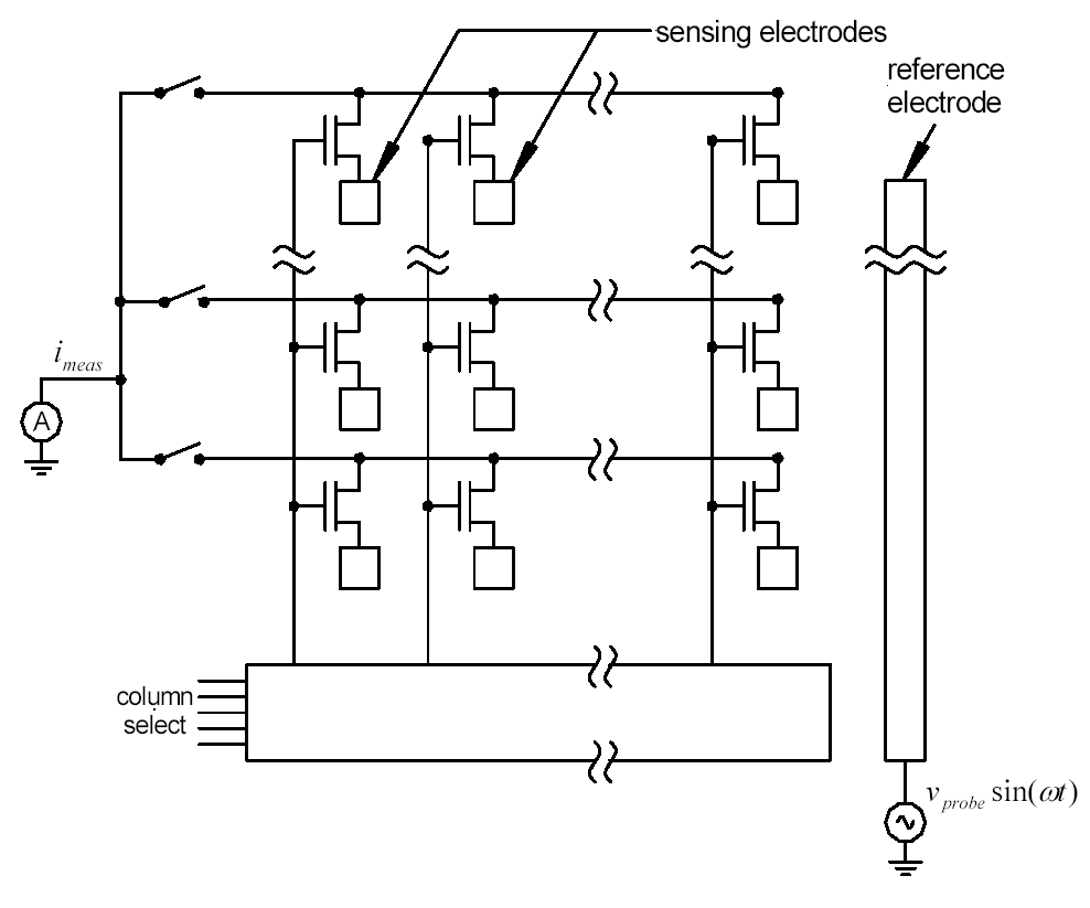
Active matrix array schematic diagram.
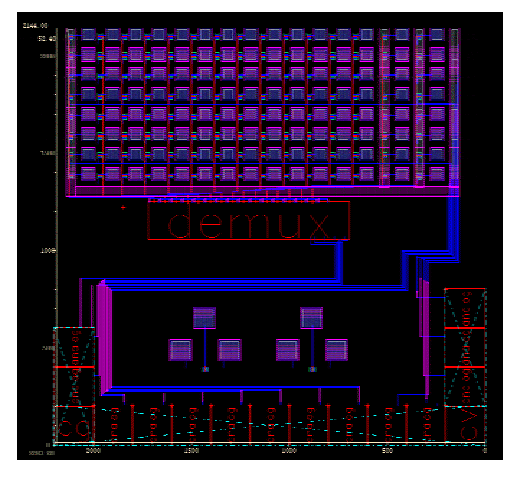
Layout of the CMOS chip.
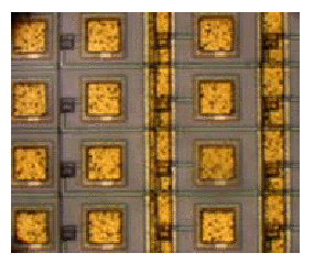
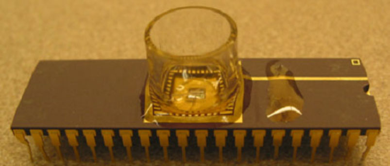
Photograph of gold-coated sensing
electrodes.
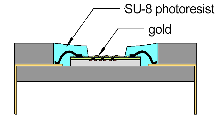
Chip in package with
passivated bond wires and pads.